Rev. 4235E≠8051≠04/04
1
Features
∑
80C52 Compatible
≠ 8051 Instruction Compatible
≠ Six 8-bit I/O Ports (64 Pins or 68 Pins Versions)
≠ Four 8-bit I/O Ports (44 Pins Version)
≠ Three 16-bit Timer/Counters
≠ 256 Bytes Scratch Pad RAM
≠ 9 Interrupt Sources with 4 Priority Levels
∑
Integrated Power Monitor (POR/PFD) to Supervise Internal Power Supply
∑
ISP (In-System Programming) Using Standard V
CC
Power Supply
∑
2048 Bytes Boot ROM Contains Low Level Flash Programming Routines and a Default
Serial Loader
∑
High-speed Architecture
≠ In Standard Mode:
40 MHz (Vcc 2.7V to 5.5V, both Internal and external code execution)
60 MHz (Vcc 4.5V to 5.5V and Internal Code execution only)
≠ In X2 mode (6 Clocks/machine cycle)
20 MHz (Vcc 2.7V to 5.5V, both Internal and external code execution)
30 MHz (Vcc 4.5V to 5.5V and Internal Code execution only)
∑
64K Bytes On-chip Flash Program/Data Memory
≠ Byte and Page (128 Bytes) Erase and Write
≠ 100k Write Cycles
∑
On-chip 1792 bytes Expanded RAM (XRAM)
≠ Software Selectable Size (0, 256, 512, 768, 1024, 1792 Bytes)
≠ 768 Bytes Selected at Reset for T89C51RD2 Compatibility
∑
On-chip 2048 Bytes EEPROM Block for Data Storage (AT89C51ED2 Only)
≠ 100K Write Cycles
∑
Dual Data Pointer
∑
Variable Length MOVX for Slow RAM/Peripherals
∑
Improved X2 Mode with Independent Selection for CPU and Each Peripheral
∑
Keyboard Interrupt Interface on Port 1
∑
SPI Interface (Master/Slave Mode)
∑
8-bit Clock Prescaler
∑
16-bit Programmable Counter Array
≠ High Speed Output
≠ Compare/Capture
≠ Pulse Width Modulator
≠ Watchdog Timer Capabilities
∑
Asynchronous Port Reset
∑
Full-duplex Enhanced UART with Dedicated Internal Baud Rate Generator
∑
Low EMI (Inhibit ALE)
∑
Hardware Watchdog Timer (One-time Enabled with Reset-Out), Power-off Flag
∑
Power Control Modes: Idle Mode, Power-down Mode
∑
Single Range Power Supply: 2.7V to 5.5V
∑
Industrial Temperature Range (-40 to +85
∞
C)
∑
Packages: PLCC44, VQFP44, PLCC68, VQFP64, PDIL40
Description
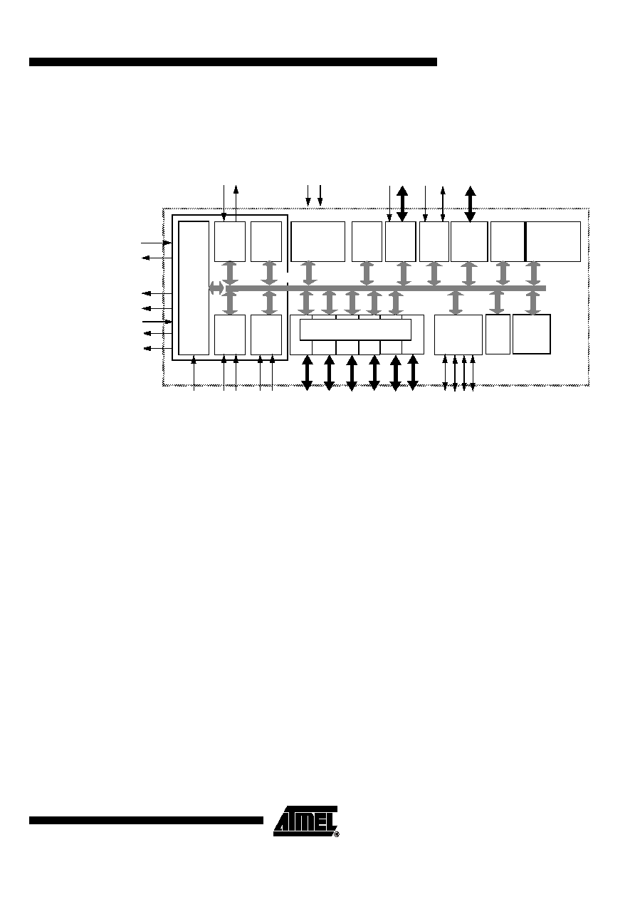
AT89C51RD2/ED2 is high performance CMOS Flash version of the 80C51 CMOS sin-
gle chip 8-bit microcontroller. It contains a 64-Kbyte Flash memory block for code and
for data.
The 64-Kbytes Flash memory can be programmed either in parallel mode or in serial
mode with the ISP capability or with software. The programming voltage is internally
generated from the standard V
CC
pin.
8-bit Flash
Microcontroller
AT89C51RD2
AT89C51ED2
2
AT89C51RD2/ED2
4235E≠8051≠04/04
The AT89C51RD2/ED2 retains all of the features of the Atmel 80C52 with 256 bytes of
internal RAM, a 9-source 4-level interrupt controller and three timer/counters. The
AT89C51ED2 provides 2048 bytes of EEPROM for nonvolatile data storage.
In addition, the AT89C51RD2/ED2 has a Programmable Counter Array, an XRAM of
1792 bytes, a Hardware Watchdog Timer, SPI interface, Keyboard, a more versatile
serial channel that facilitates multiprocessor communication (EUART) and a speed
improvement mechanism (X2 Mode).
The fully static design of the AT89C51RD2/ED2 allows to reduce system power con-
sumption by bringing the clock frequency down to any value, including DC, without loss
of data.
The AT89C51RD2/ED2 has 2 software-selectable modes of reduced activity and an 8-
bit clock prescaler for further reduction in power consumption. In the Idle mode the CPU
is frozen while the peripherals and the interrupt system are still operating. In the Power-
down mode the RAM is saved and all other functions are inoperative.
The added features of the AT89C51RD2/ED2 make it more powerful for applications
that need pulse width modulation, high speed I/O and counting capabilities such as
alarms, motor control, corded phones, and smart card readers.
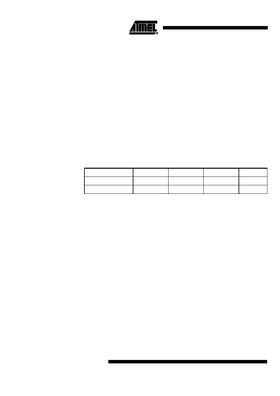
Table 1. Memory Size and I/O Pins
Package
Flash (Bytes)
XRAM (Bytes)
Total RAM (Bytes)
I/O
PLCC44/VQFP44/DIL40
64K
1792
2048
34
PLCC68/VQFP64
64K
1792
2048
50

4
AT89C51RD2/ED2
4235E≠8051≠04/04
SFR Mapping
The Special Function Registers (SFRs) of the AT89C51RD2/ED2 fall into the following
categories:
∑
C51 core registers: ACC, B, DPH, DPL, PSW, SP
∑
I/O port registers: P0, P1, P2, P3, PI2
∑
Timer registers: T2CON, T2MOD, TCON, TH0, TH1, TH2, TMOD, TL0, TL1, TL2,
RCAP2L, RCAP2H
∑
Serial I/O port registers: SADDR, SADEN, SBUF, SCON
∑
PCA (Programmable Counter Array) registers: CCON, CCAPMx, CL, CH, CCAPxH,
CCAPxL (x: 0 to 4)
∑
Power and clock control registers: PCON
∑
Hardware Watchdog Timer registers: WDTRST, WDTPRG
∑
Interrupt system registers: IE0, IPL0, IPH0, IE1, IPL1, IPH1
∑
Keyboard Interface registers: KBE, KBF, KBLS
∑
SPI registers: SPCON, SPSTR, SPDAT
∑
BRG (Baud Rate Generator) registers: BRL, BDRCON
∑
Clock Prescaler register: CKRL
∑
Others: AUXR, AUXR1, CKCON0, CKCON1
5
AT89C51RD2/ED2
4235E≠8051≠04/04
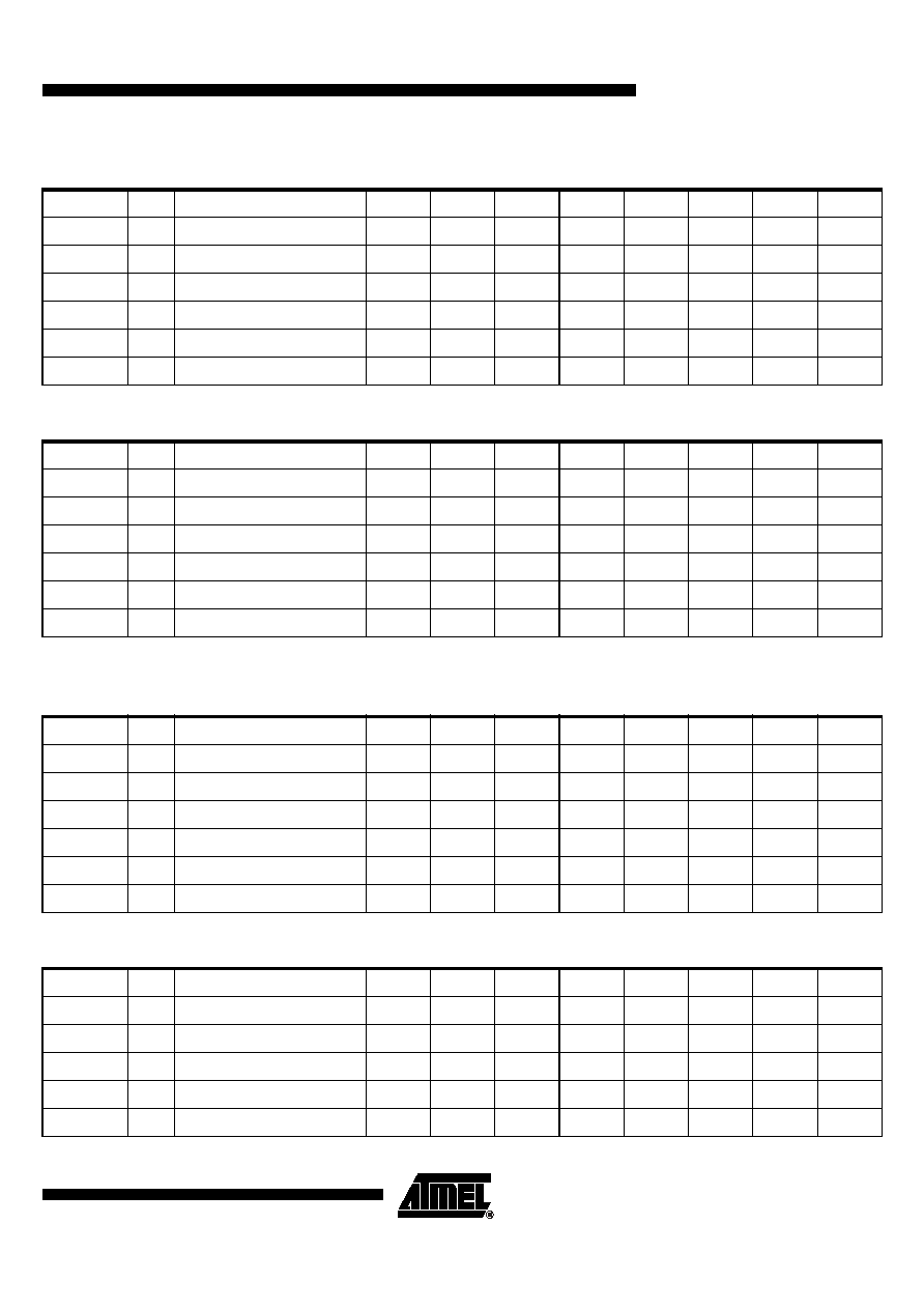
Table 2. C51 Core SFRs
Mnemonic
Add
Name
7
6
5
4
3
2
1
0
ACC
E0h
Accumulator
B
F0h
B Register
PSW
D0h
Program Status Word
CY
AC
F0
RS1
RS0
OV
F1
P
SP
81h
Stack Pointer
DPL
82h
Data Pointer Low Byte
DPH
83h
Data Pointer High Byte
Table 3. System Management SFRs
Mnemonic
Add
Name
7
6
5
4
3
2
1
0
PCON
87h
Power Control
SMOD1
SMOD0
-
POF
GF1
GF0
PD
IDL
AUXR
8Eh
Auxiliary Register 0
DPU
-
M0
XRS2
XRS1
XRS0
EXTRAM
AO
AUXR1
A2h
Auxiliary Register 1
-
-
ENBOOT
-
GF3
0
-
DPS
CKRL
97h
Clock Reload Register
-
-
-
-
-
-
-
-
CKCKON0
8Fh
Clock Control Register 0
-
WDTX2
PCAX2
SIX2
T2X2
T1X2
T0X2
X2
CKCKON1
AFh
Clock Control Register 1
-
-
-
-
-
-
-
SPIX2
Table 4. Interrupt SFRs
Mnemonic
Add
Name
7
6
5
4
3
2
1
0
IEN0
A8h
Interrupt Enable Control 0
EA
EC
ET2
ES
ET1
EX1
ET0
EX0
IEN1
B1h
Interrupt Enable Control 1
-
-
-
-
-
ESPI
KBD
IPH0
B7h
Interrupt Priority Control High 0
-
PPCH
PT2H
PHS
PT1H
PX1H
PT0H
PX0H
IPL0
B8h
Interrupt Priority Control Low 0
-
PPCL
PT2L
PLS
PT1L
PX1L
PT0L
PX0L
IPH1
B3h
Interrupt Priority Control High 1
-
-
-
-
-
SPIH
KBDH
IPL1
B2h
Interrupt Priority Control Low 1
-
-
-
-
-
SPIL
KBDL
Table 5. Port SFRs
Mnemonic
Add
Name
7
6
5
4
3
2
1
0
P0
80h
8-bit Port 0
P1
90h
8-bit Port 1
P2
A0h
8-bit Port 2
P3
B0h
8-bit Port 3
P4
C0h
8-bit Port 4